Strengthen The Industrial Use Of Chiplets In Germany
Germany has taken a significant step forward in semiconductor innovation with the official launch of the Chiplet Application Hub by the Research Fab Microelectronics Germany (FMD) on March 31, 2025, at Hannover Messe. This initiative represents a strategic move to advance Germany’s position in chiplet technology and strengthen its semiconductor ecosystem.
The Strategic Importance of Chiplet Technology
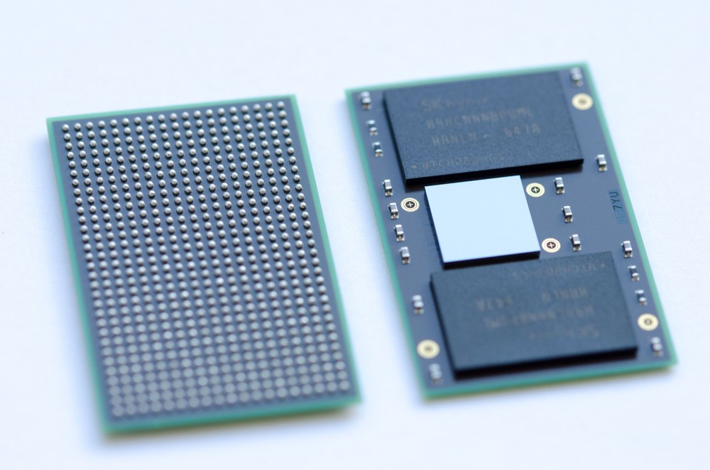
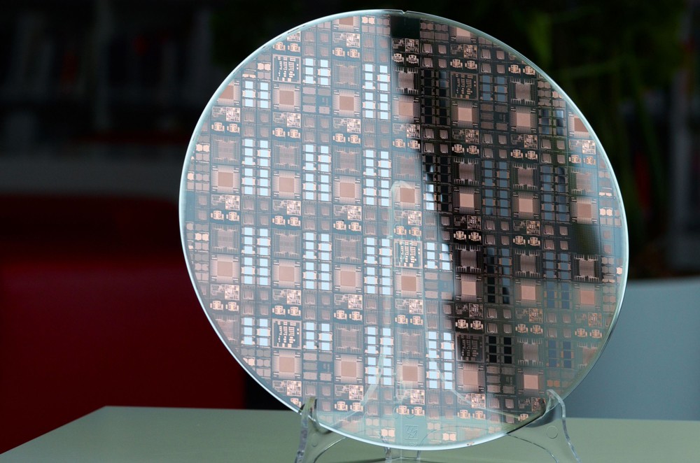
Chiplet technology has emerged as a cornerstone innovation in modern microelectronics, enabling modular and scalable semiconductor integration. Unlike traditional monolithic designs, chiplets allow different technological components to be combined on a single package, tailored to specific applications. This modular approach offers greater flexibility, improved energy efficiency, and enhanced performance across various domains.
For Germany, mastering chiplet technology represents not just technological advancement but economic resilience. As global semiconductor supply chains face increasing challenges, developing domestic capabilities in advanced packaging and heterogeneous integration becomes critical for maintaining technological sovereignty and industrial competitiveness.
The Chiplet Application Hub: A Catalyst for Innovation
The newly established Chiplet Application Hub serves as a central platform for the development and application of chiplet technologies in Germany. Building on the infrastructure of the APECS (Advanced Packaging and Heterogeneous Integration for Electronic Components and Systems) pilot line launched in late 2024, the hub creates a bridge between cutting-edge research and industrial applications.
With substantial funding – the APECS initiative alone received €730 million in total funding – the hub is well-positioned to drive meaningful innovation. Its primary mission is to accelerate the development and deployment of “chiplets made in Germany,” working closely with industry partners to bring laboratory discoveries to market-ready solutions.
Industry Applications and Economic Impact
The Chiplet Application Hub’s work will have far-reaching implications across multiple sectors:
Automotive Industry
For Germany’s powerhouse automotive sector, chiplet technology enables more centralized and powerful control units, flexible integration across vehicle categories, and improved energy efficiency. As vehicles become increasingly software-defined, the demand for sophisticated semiconductor solutions grows proportionately.
Jürgen Heckelmann, Head of Strategic Semiconductor Management at Audi AG, and Andreas Aal from Volkswagen Commercial Vehicles have recognized the potential of chiplet-based systems to enable flexibility, energy efficiency, and design scalability in automotive electronics.
High-Performance Computing and AI
The modular integration of semiconductor components through chiplet technology creates more powerful and energy-efficient computing solutions. Dr. Heike Riel of IBM has highlighted this as “a crucial building block for the future of the semiconductor industry,” particularly for applications in artificial intelligence and data processing.
Industrial Electronics and Medical Devices
Beyond automotive and computing, chiplet technology offers advantages for industrial electronics and medical devices. Advanced packaging and the integration of high-performance subsystems support the development of more capable sensor modules, edge computing devices, and specialized control units.
European Collaboration and Technological Resilience
The Chiplet Application Hub doesn’t operate in isolation but forms part of a broader European strategy. It complements FMD’s role in the Chips for Europe Initiative and supports the implementation of the EU Chips Act in Germany.
A significant development in this European ecosystem is the planned arrival of Belgium’s imec research institution, which will establish a research group in Heilbronn, Baden-Württemberg. Focusing on chiplet architectures for high-performance computing in the automotive sector, this collaboration demonstrates cross-border coordination in action.
The memorandum of understanding (MoU) between imec and FMD outlines a shared strategic direction to maximize the potential of chiplet technologies, reinforcing their joint commitment to driving innovation and setting new standards for development and industrial use.
From Research to Industrial Implementation
What distinguishes the Chiplet Application Hub is its emphasis on the entire innovation cycle – from research and design to prototyping and scalable deployment. By providing industry partners with access to state-of-the-art facilities and expertise, the hub accelerates the transition from theoretical concepts to practical applications.
This structured path from research to industrial use is essential for strengthening Germany’s technological resilience. As Prof. Albert Heuberger, founding director of the Chiplet Application Hub, emphasizes, it represents “a vital asset for implementing the EU Chips Act in Germany” and will be closely linked to competence centers being established across Europe.
Looking Ahead: Germany’s Semiconductor Future
The establishment of the Chiplet Application Hub marks a significant milestone in Germany’s semiconductor strategy. By fostering collaboration between research institutions and industry partners, it creates a foundation for sustainable innovation in chiplet technologies.
As global demand for advanced semiconductor solutions continues to grow, Germany’s investment in chiplet research and development positions it to play a leading role in shaping the future of microelectronics. The hub’s focus on practical, application-driven solutions ensures that technological advancements will translate into tangible benefits for German industry and the broader economy.
Through initiatives like the Chiplet Application Hub, Germany is not just strengthening its industrial use of chiplets but reinforcing its position as a key player in the global semiconductor landscape.