Lightmatter’s New Products Enable Interconnection Support for Thousands of GPUs
Nicholas Harris founded a company called Lightmatter in California, USA. Recently, Lightmatter announced a series of new products that could revolutionize AI infrastructure.

Breakthrough Photonic Technologies for Next-Generation AI
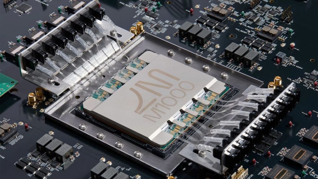
The first new product announced is the Passage M1000 photonic superchip (referred to as “M1000”), which the company claims delivers the world’s fastest AI interconnection. It employs breakthrough 3D photonic interconnect layer technology, providing maximum bandwidth and the largest chip complex for next-generation AI infrastructure silicon designs.
The second product is the Passage L200 co-packaged optical device (referred to as “L200”). The L200 extends bandwidth across the entire chip area through the world’s first edge-free I/O. The company states this is the fastest co-packaged optical device in the AI field, and its revolutionary 3D photonic interconnect solution eliminates bandwidth bottlenecks, accelerating AI model training speed by 8 times.
Nick Harris, Lightmatter’s founder and CEO, said: “Bandwidth scaling has become a critical barrier to AI development. The engineering breakthrough represented by the L200 series 3D co-packaged optical solution provides the fundamental building blocks for next-generation AI processors and switches.”
Without doubt, Lightmatter aims to reshape how chips communicate and compute using photonic computing technology. The MIT website praised these products in a press release, stating that they accelerate the progress toward light-speed computing.
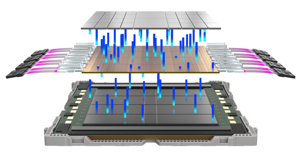
M1000: Interconnection Support for Thousands of GPUs in a Single Domain
The M1000 is a 3D photonic superchip designed for next-generation XPUs (X Processing Units) and switches, providing 114 Tbps of total optical bandwidth for demanding AI infrastructure applications. The M1000 benchmark platform covers an area exceeding 4,000 square millimeters, functioning as a multi-mask active photonic interposer. Based on this platform, it’s possible to build the world’s largest 3D packaged bare chip complex, supporting interconnection for thousands of GPUs in a single domain.
In existing chip designs, the interconnection bandwidth between processors, memory, and I/O chiplets is limited because electrical I/O connections are restricted to the edges of these chips. The M1000 overcomes this limitation by enabling electro-optical I/O release at almost any location on its surface for stacked chip complexes.
The M1000 achieves full-domain interposer interconnection through a massively reconfigurable waveguide network that transmits high-bandwidth wavelength division multiplexing (WDM) optical signals across the entire platform. It features fully integrated fiber interfaces, supporting a breakthrough configuration of up to 256 fibers. Compared to traditional co-packaged optics (CPO) and similar solutions, this allows the M1000 to achieve an order of magnitude improvement in bandwidth performance within a smaller package size.
Currently, Lightmatter is working closely with companies including GlobalFoundries and Amkor to achieve mass production of the M1000. The M1000 employs GlobalFoundries’ Fotonix silicon photonics platform technology, which enables a mass-producible design solution that can scale with AI demands by seamlessly integrating photonic components with high-performance CMOS logic on a single die. The M1000 is expected to launch in summer 2025, alongside the company’s optical engine, Guide.
L200: World’s First 3D Co-Packaged Optical Product
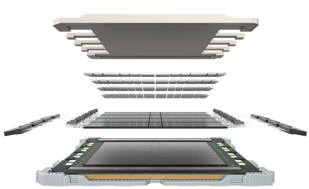
The second product launched, the L200, is described by Lightmatter as the world’s first 3D co-packaged optical product. The L200 is designed to integrate with the latest XPU and switch chip designs, enabling AI performance scaling by eliminating interconnection bandwidth bottlenecks.
The L200 3D co-packaged optical series includes two versions: 32Tbps and 64Tbps, offering 5 to 10 times better performance compared to existing solutions, bringing the total I/O bandwidth per chip package to over 200Tbps.
Current bandwidth scaling lags far behind computational performance improvements. Continued advancement in AI computing requires fundamental changes in interconnection technology. Current connection solutions, including electrical, optical, and traditional co-packaged optics, are limited by bandwidth because their I/O interfaces are restricted to the edges of the chip.
The L200 overcomes these limitations through the world’s first edge-free I/O, extending bandwidth across the entire chip area. This modular 3D co-packaged optical solution utilizes universal chiplet interconnect technology die-to-die (D2D) interfaces and facilitates seamless integration of scalable chiplet-based architectures with next-generation XPUs and switches.
The L200 3D co-packaged optics integrates Alphawave Semi’s latest chiplet technology, combining universal chiplet interconnect interfaces with optical communication-ready serializers/deserializers and Lightmatter’s photonic integrated circuit technology. Alphawave Semi’s advanced node electronic integrated circuits use standard wafer-on-chip technology and are 3D integrated onto the photonic integrated circuit. This 3D integration technology allows serializer/deserializer I/O to be placed anywhere on the chip, not just at its edges, providing each L200 with bandwidth equivalent to 40 pluggable optical transceivers. Additionally, multiple L200s can be integrated within a single package, enabling wide application in XPU and switch applications.
The L200 features advanced redundancy and resilience designs and is equipped with Lightmatter’s Guide optical engine. Each module provides exceptional laser integration and total optical power, supporting the full bandwidth of the L200.
Lightmatter currently offers two product models: the L200 (32Tbps) and L200X (64Tbps) 3D co-packaged optical engines. These solutions are based on Lightmatter’s proven Passage technology platform, providing 16 wavelength division multiplexing wavelengths per waveguide/fiber, with state-of-the-art and fully integrated photonic control capabilities.
The L200 is specifically designed for mass production, with silicon photonics factory and outsourced assembly and test partners including GlobalFoundries, ASE Semiconductor, and Amkor. Lightmatter’s L200 and L200X 3D co-packaged optical chips will be available in 2026, aimed at accelerating the time-to-market and performance enhancement of next-generation XPUs and switches required for next-generation foundational AI models.
Andrew Schmitt, founder and chief analyst at Cignal AI, commented: “AI data center interconnects face growing bandwidth and power consumption challenges. Co-packaged optics—directly integrating optical devices into XPUs and switches—is the inevitable solution. Lightmatter’s bold approach provides the essential elements of co-packaged optics and offers hyperscale data center operators and chip manufacturers a path to high-performance systems.”
Urgent Market Demand for Photonic Chips
Currently, human ability to integrate increasingly smaller transistors into chips has enabled today’s ubiquitous computing era. However, this approach is finally approaching its limits, with some experts declaring that Moore’s Law and the related Dennard’s Scaling are coming to an end. The timing of these technical bottlenecks couldn’t be worse. In recent years, computational demands, especially for AI, have grown exponentially with no signs of slowing down.
Meanwhile, for decades, people have hoped to develop optical chips that use photons instead of electrons for computing tasks. Optical chips offer the advantages of faster speed and lower energy consumption. However, making them actually work has not been easy.
In 2017, Harris, along with colleagues including Yi Chen Shen, published the aforementioned paper in Nature. In the paper, they used an optical chip approach to calculate the output results of a neural network trained through traditional methods. They described a “light path” consisting of 56 programmable interferometer devices that could decompose and reconstruct light waves. This method solved the problem of correctly identifying vowels, distinguishing three-quarters of the vowels in 180 cases. Although this result temporarily fell short of the over 90% recognition accuracy of ordinary computers, the circuit’s performance was still impressive.
Shortly thereafter, Harris and Shen Yi Chen founded their respective startups in the United States and China. Once such neural networks can be functionally implemented and trained on optical chips, some inference processes, such as identifying sounds corresponding to vowels, would flow as smoothly as photons through the chip, while also offering high speed and energy efficiency.
Before entering MIT for his PhD, Harris worked at the semiconductor company Micron Technology, researching the basic devices behind integrated chips. This experience made him realize that the traditional method of improving computer performance by cramming more transistors onto each chip had reached its limit. At that time, he saw that the computing roadmap was slowing down and wanted to figure out how to continue advancing it.
So, what methods could enhance computer performance? Quantum computing and photonics are two paths. Harris came to MIT to pursue a PhD under the guidance of Dirk Englund, an associate professor in the Department of Electrical Engineering and Computer Science, researching photonic quantum computing. As part of his doctoral work, he built silicon-based integrated photonic chips that could send and process information using light rather than electricity. This work led to dozens of patent applications and over 80 research papers published in prestigious journals like Nature.
But at MIT, another technology caught Harris’s attention. “I remember walking down the hall and seeing students pouring out of these auditorium-sized classrooms, watching livestreamed lecture videos, listening to professors teaching deep learning,” Harris told media. “Everyone on campus knew deep learning was going to be a big deal, so I started learning more about it, and we realized that the system I was building for photonic quantum computing could actually be used for deep learning.”
Harris had originally planned to become a professor after obtaining his PhD, but he realized that entrepreneurship could attract more funding and enable faster innovation. So he teamed up with Darius Bunandar (a 2019 MIT PhD graduate who also studied in Englund’s lab) and Thomas Graham (a 2018 MIT MBA graduate). These three co-founders successfully entered the entrepreneurial field after winning the $100,000 MIT Entrepreneurship Competition in 2017.