UALink 1.0 Specification Released: The Beginning of a Challenge to NVIDIA’s AI Dominance
Introduction: A New Era in AI Computing Interconnect
The Ultra Accelerator Link (UALink) 1.0 specification has been officially released, marking the beginning of new competition in the artificial intelligence (AI) and high-performance computing (HPC) sectors. This open, high-speed, low-latency interconnect standard is jointly promoted by industry giants including AMD, Broadcom, Google, and Intel, directly challenging NVIDIA’s dominant position with its proprietary NVLink technology.
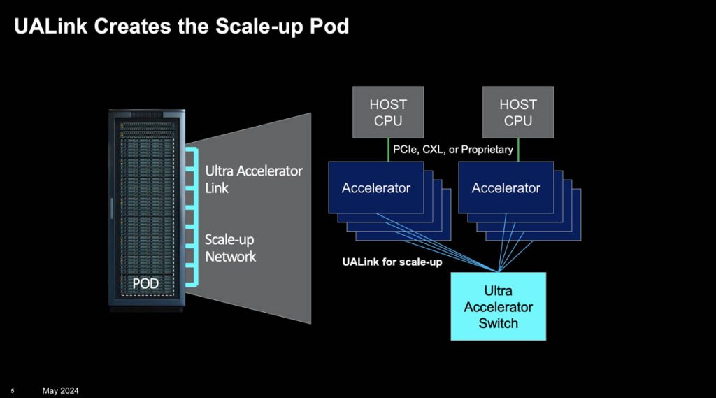
UALink 1.0 supports bandwidth of 200 GT/s per channel and can connect up to 1024 accelerators. It features low cost, scalability, and high security, injecting new competitive vitality into the AI accelerator ecosystem.
This article will analyze the significance of UALink from both technical innovation and market competition perspectives, exploring its potential impact on the AI industry landscape.
Technical Innovations and Advantages of UALink
The birth of UALink stems from a collective response by AMD, Broadcom, Intel, and others to NVIDIA’s proprietary NVLink technology.
NVIDIA has built an efficient GPU interconnect ecosystem through NVLink and NVSwitch, demonstrating powerful performance especially in rack-level solutions like Blackwell NVL72. However, the closed nature of NVLink limits participation from other manufacturers and increases system integration costs.
UALink breaks this barrier through an open standard, allowing seamless collaboration between accelerators from different manufacturers (such as AMD Instinct GPUs and Intel Gaudi), reducing the complexity and cost of data center deployments.
This construction of an open ecosystem not only provides flexibility for system integrators and data center operators but also creates opportunities for small and medium-sized AI hardware manufacturers to participate in the competition.
UALink Protocol Architecture
The UALink 1.0 protocol stack consists of physical, data link, transaction, and protocol layers, deeply optimized for AI and HPC workloads:
- Physical Layer: Based on standard Ethernet components (such as 200GBASE-KR1/CR1), with improved forward error correction (FEC) and codeword interleaving techniques to significantly reduce latency while maintaining compatibility with existing Ethernet ecosystems.
- Data Link Layer: Employs a flit packaging mechanism from 64 bytes to 640 bytes, combined with cyclic redundancy check (CRC) and optional retry logic to ensure reliability and efficiency of data transmission.
- Transaction Layer: Achieves up to 95% protocol efficiency through compressed addressing and direct memory operations (read, write, atomic transactions), optimizing cross-accelerator memory access, particularly suitable for the stringent low-latency requirements in AI training and inference.
- Protocol Layer: Supports UALinkSec hardware-level encryption and trusted execution environments (such as AMD SEV, Intel TDX), providing secure isolation and confidential computing capabilities for multi-tenant data centers.
Performance and Scalability
This layered design simplifies protocol complexity while maintaining high performance. Compared to PCI-Express (PCIe) or CXL, UALink offers advantages in bandwidth and latency, particularly suitable for large-scale AI computing clusters.
UALink supports connecting up to 1024 accelerators, covering 1 to 4 racks, with a single-channel bidirectional bandwidth of 200 GT/s, reaching 800 GT/s in a four-channel configuration.
This scalability capability enables it to address the growing demands of AI models, such as training and inference tasks for large language models (LLMs).
Additionally, UALink’s round-trip latency is less than 1 microsecond with 64B/640B payloads, and port-to-port hop latency is approximately 100-150 nanoseconds, approaching the performance of PCIe switches and far superior to traditional Ethernet. This low-latency characteristic is crucial for building AI computing Pods with deterministic performance.
Energy Efficiency and Cost Optimization
UALink’s design emphasizes energy efficiency, with its switches consuming only 1/3 to 1/2 the power of equivalent Ethernet ASICs, saving 150-200 watts of power per accelerator. Smaller chip area and lower power consumption not only reduce hardware costs but also decrease data center power and cooling expenses, optimizing total cost of ownership (TCO).
This is particularly important for hyperscale cloud service providers who need to balance performance with operational costs.
UALink Challenging NVIDIA’s Ecosystem Barriers
NVIDIA’s dominance in the AI accelerator market stems not only from its powerful GPU hardware but also from the synergy of NVLink, NVSwitch, and the CUDA software ecosystem.
For example, the Blackwell NVL72 rack connects 72 GPUs through NVLink, with Pod-level expansion supporting 576 GPUs, while the upcoming Vera Rubin platform will further increase the number of GPUs per rack to 144.
In comparison, UALink 1.0 theoretically supports a Pod scale of 1024 accelerators, showing greater expansion potential.
However, NVIDIA’s ecosystem barrier is not just about hardware interconnection; the widespread adoption of CUDA and optimized toolchains have made it deeply rooted in the developer community.
The UALink alliance needs to compete not only at the hardware level but also promote the maturity of software ecosystems (such as ROCm, oneAPI) to attract developers to migrate from the NVIDIA platform.
Industry Alliance and Product Deployment
The UALink alliance members span multiple domains including chip design (AMD, Intel, Broadcom), cloud services, network equipment (Cisco), and system integration (HPE).
This broad industry support provides a foundation for the rapid implementation of UALink. For example, Synopsys has launched UALink IP controllers and verification IP, while Astera Labs and Broadcom also plan to produce UALink switches.
However, interest coordination within the alliance may be a major challenge. For instance, Google and Meta focus on custom accelerators (such as TPUs), while AMD and Intel hope to promote general-purpose GPUs. Differences in priorities among members may lead to complexity in standard evolution.
Furthermore, NVIDIA’s absence makes it difficult for UALink to shake its market dominance in the short term, especially in the high-end AI training market.
Implementation Timeline and Market Challenges
The release of the UALink 1.0 specification marks significant progress in technical development, but it typically takes 12-18 months from specification to commercial products. The alliance expects the first UALink devices to be available in 2026, while NVIDIA’s NVLink 6.0 and Rubin Ultra platform may further enhance performance by 2027.
This means UALink needs to prove its performance and cost advantages within a limited time window to capture market share.
Market acceptance will depend on performance in actual deployments, such as whether it can seamlessly integrate with existing data center infrastructure and significantly reduce the overall cost of AI training and inference.
Additionally, small and medium-sized enterprises may be more receptive to open standards than large customers who rely on the NVIDIA ecosystem, providing an opportunity for UALink to enter the market.
Collaboration with Ultra Ethernet Consortium
Collaboration with the Ultra Ethernet Consortium (UEC) is an important component of UALink’s strategy.
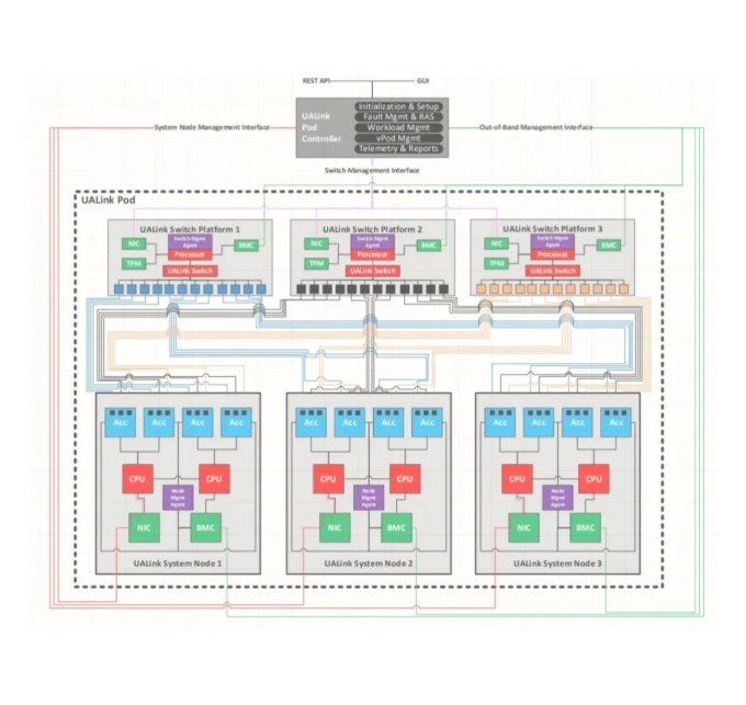
UEC is dedicated to optimizing Ethernet to meet the scaling needs of AI and high-performance computing, while UALink focuses on high-speed interconnection of accelerators within Pods. The combination of the two is expected to form a complete “scale-in + scale-out” solution. For example, UALink can be used to connect Pods of 8-128 servers, while Ultra Ethernet can achieve cross-Pod scaling.
This synergy enhances UALink’s ecosystem competitiveness but also increases the complexity of technology integration, requiring the alliance to maintain efficient collaboration in standard setting and product development.
Conclusion: Reshaping the AI Industry Landscape
The release of the UALink 1.0 specification symbolizes the evolution of the AI industry’s competitive landscape. As an open standard, UALink provides AMD, Intel, Google, and others with a key weapon to challenge NVIDIA’s AI dominance through high-speed, low-latency, and low-cost interconnect technology.
The optimized design of the protocol stack, scalability, and security lay the foundation for building next-generation AI computing Pods, while the potential synergy with Ultra Ethernet further enhances its market prospects. The alliance needs to continue its efforts in software ecosystems, product implementation, and market promotion, especially to prove its value within the critical time window of 2026.
From a broader perspective, the emergence of UALink reflects the AI industry’s demand for openness and diversity. With the continued growth of AI training and inference demands, the competition between UALink and NVLink will ignite immediately.