SoC Chip Design – AI Accelerator Interconnect Technology Analysis
1. Overview of AI Accelerator Interconnect Technologies
AI accelerator interconnect technologies serve as the core for efficient data transmission and computational resource coordination, especially in high-performance computing, data centers, and distributed computing. Key interconnect technologies include various solutions that help achieve exceptional performance.
PCIe (Peripheral Component Interconnect Express), as a top-tier high-speed interface standard, is widely used for connecting computer peripherals and is particularly suitable for AI accelerator cards. The new generation PCIe 4.0 and PCIe 5.0 achieve ultra-high bandwidths of 16 GT/s and 32 GT/s respectively, perfectly meeting the stringent high-speed data transmission requirements of AI accelerators. With excellent versatility and widespread support, PCIe has become the preferred technology for accelerator connections, leading new trends in the computing field.
NVLink, NVIDIA’s innovation, is specifically designed for high-speed, low-latency communication between GPUs and with CPUs. Its bandwidth far exceeds PCIe, greatly improving parallel computing and data sharing efficiency in multi-GPU systems, making it a revolutionary technology in the high-performance computing field.
NVSwitch, meticulously crafted by NVIDIA, is a switching technology tailored for multi-GPU systems, building high-speed interconnection networks between GPUs. This technology enables full-bandwidth communication, significantly enhancing large-scale parallel computing efficiency and leading multi-GPU performance to new heights.
CXL is an emerging open industry standard led by Intel, optimizing interconnection between CPUs and accelerators, memory expansion devices. It supports advanced features such as memory sharing and cache coherency, particularly suitable for accelerating AI computing, leading computing performance to new heights.
AMD’s Infinity Fabric technology, as a leading on-chip and inter-chip interconnect solution, seamlessly connects CPUs, GPUs, and various accelerators. On the AMD Instinct MI300X platform, this technology integrates multiple GPU modules, significantly enhancing system data exchange efficiency, bringing a qualitative leap to computing performance.
UALink: Ultra Accelerator Link (UALink) is also a high-speed accelerator interconnect technology that can improve the performance of next-generation AI/ML clusters. Eight founding manufacturers (like the Super Ethernet Alliance, NVIDIA is not seen in the UALink alliance) have also established an open industry standard organization to formulate relevant technical specifications to promote breakthrough performance required by new usage models while supporting the development of an open ecosystem for data center accelerators.
Companies including AMD, Broadcom, Cisco, Google, Hewlett Packard Enterprise (HPE), Intel, Meta, and Microsoft have announced they have developed a new interconnect technology called UALink (Ultra Accelerator Link) for AI data center networks. By establishing an open standard for communication between AI accelerators, they aim to break the monopoly of market leader NVIDIA.
Optimization of interconnect technologies, especially for AI applications, is key to breaking through data transmission bottlenecks, improving computing efficiency, and promoting the integration of heterogeneous computing architectures. Facing increasingly complex AI models and workloads, efficient, low-latency interconnect solutions are becoming increasingly indispensable.
2. PCIe
PCIe (Peripheral Component Interconnect Express) is a high-speed serial computer expansion bus standard, connecting motherboards with hardware such as graphics cards, solid-state drives, network cards, etc. Since its release in 2003, PCIe has evolved to PCIe 3.0, PCIe 4.0, and PCIe 5.0 is gradually becoming widespread. Its key features include high bandwidth and low latency, providing powerful momentum for modern computing. Whether for AI acceleration or data processing, PCIe demonstrates excellent performance, driving rapid technological development.
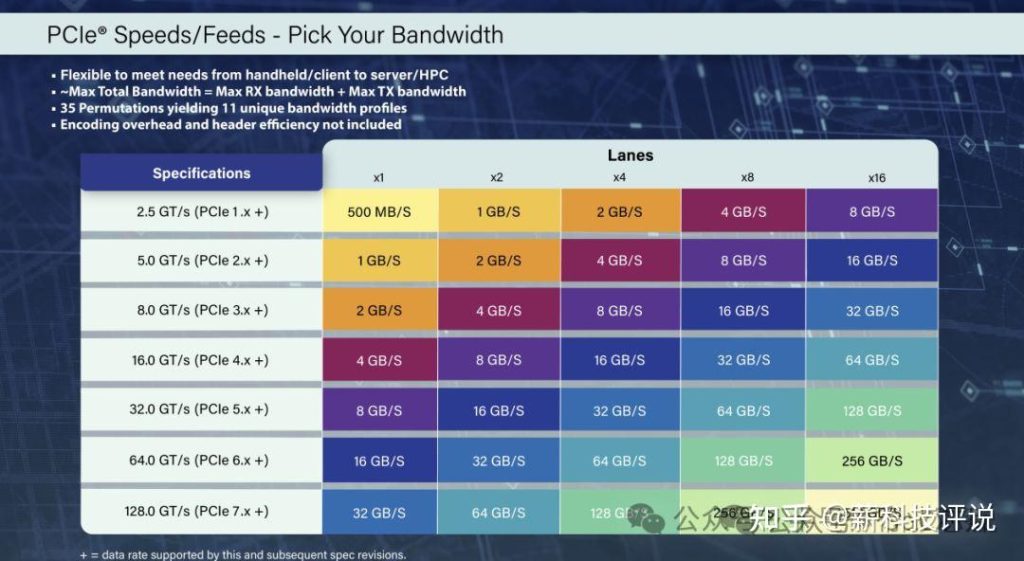
The PCIe standard continuously refreshes data transfer speeds. PCIe 3.0 channel rates reach 8GT/s, PCIe 4.0 doubles to 16GT/s, and PCIe 5.0 doubles again to an impressive 32GT/s. Each PCIe slot can be configured with 1 to 16 channels, with bandwidth increasing proportionally with the number of channels. High-speed transmission helps you easily handle big data challenges and unleash unlimited potential.
- Excellent compatibility: New PCIe standard devices are compatible with old slots, ensuring backward compatibility, but speeds are limited by the maximum rate of the old standard, ensuring stable operation. PCIe, with its excellent performance and wide applicability, has become the industry standard for high-performance peripheral connections, widely supported in modern computer systems, achieving seamless integration.
PCIe interfaces play a crucial role in meeting the needs of data-intensive applications in fields such as AI acceleration, high-performance computing, graphics processing, and storage solutions, thanks to their high-rate characteristics. With technological innovation, the evolution of PCIe standards is essential for achieving future high data transfer rates and low latency, especially in cutting-edge fields such as cloud computing, data centers, and high-performance computing, its impact cannot be underestimated.
In early April 2024, PCI-SIG released version 0.5 of the PCI-Express 7.0 specification, the second draft, marking the final stage for members to submit features for the new standard. PCI-SIG reaffirmed with this update that the development of the new standard is progressing steadily, with the final version expected to be released in 2025, ensuring the continuous innovation and evolution of industry technology.
PCIe 7.0 leads the revolution in next-generation computer interconnect technology. Its data transfer speed reaches 128 GT/s, doubling compared to PCIe 6.0, and increasing fourfold compared to PCIe 5.0. The 16-channel (x16) connection supports bi-directional 256 GB/s bandwidth with no encoding overhead. This leap will greatly satisfy the urgent need for high-speed data transmission in future data centers, artificial intelligence, and high-performance computing, opening a new era of data processing.
PCIe 7.0 revolutionizes data transfer rates, doubling its physical layer bus frequency, far exceeding PCIe 5.0 and 6.0. It retains PAM4 signaling, 1b/1b FLIT encoding, and FEC technology, ensuring stable and reliable data. PCI-SIG emphasizes that PCIe 7.0 focuses more on optimizing channel parameters, expanding coverage, and improving power efficiency, demonstrating its excellent performance and forward-looking design, leading a new chapter in future data transmission.
Overall, given that PCIe 7.0 needs to double the bus frequency of the physical layer, while PCIe 6.0 avoided this major development through PAM4 signaling, the engineers behind this standard have a large workload. In terms of improving data signals, nothing comes free, and for PCIe 7.0, PCI-SIG can be said to have returned to hard mode development, as it needs to improve the physical layer again—this time to make it run at around 30GHz. However, how much heavy work will be done through intelligent signal transmission (and retimers), and how much will be done through pure material improvements (such as thicker printed circuit boards (PCBs) and low-loss materials), remains to be seen.
A key milestone for PCIe 7.0 is the completion of version 0.7 specification, which is the complete draft. This version requires all aspects to be thoroughly defined and the electrical specifications to be verified through test chips. Once released, no new features will be added. Given that PCIe 6.0 went through versions 0.3 to 0.9 before being finalized, PCIe 7.0 is expected to follow a similar path towards becoming a mature standard. It is anticipated that PCIe 7.0 hardware will still need several years to reach the market after the specification is finalized in 2025. Although controller IP and initial hardware development have already started, the entire development process far exceeds the scope of specification release and still requires patience.
PCI-SIG announces that the PCIe 7.0 specification is expected to be fully released in 2025, covering functional upgrade goals and leading a new chapter in future data transmission. The x16 configuration achieves a 128 GT/s raw bit rate with a bi-directional bit rate of up to 512 GB/s, demonstrating excellent performance and meeting high-speed data transmission requirements.
- Utilizing PAM4 (4-level Pulse Amplitude Modulation) signaling;
- Continuing to achieve low latency and high reliability goals;
- Improving power efficiency;
- Maintaining backward compatibility with all previous generations of PCIe technology;
PCIe 7.0 technology is designed for data-intensive markets (such as 800G Ethernet, AI/ML, hyperscale data centers, HPC, quantum computing, and cloud), providing scalable interconnect solutions. The technology focuses on enhancing channel parameters, expanding coverage, and optimizing energy efficiency to meet high-bandwidth application needs, providing strong support for industry innovation.
3. NVLink
NVLink, NVIDIA’s high-speed interconnect technology, is specifically designed to enhance data transfer speed and efficiency between GPUs and between GPUs and CPUs, ensuring efficient and swift data transmission, leading a new era in computing performance.
NVLink’s high-speed bandwidth significantly exceeds traditional PCIe buses, bringing a performance leap to multi-GPU systems. The fourth-generation NVLink bandwidth reaches 900GB/s, seven times that of PCIe 5.0. This breakthrough is crucial for applications requiring rapid data exchange such as deep learning, high-performance computing, and big data analysis, helping the industry achieve higher efficiency and excellent performance.
NVLink achieves low latency, with point-to-point direct connections significantly reducing data transmission delays, notably accelerating communication between GPUs and between GPUs and CPUs, significantly improving system response speed and operational efficiency.
- Parallel processing optimization: NVLink technology enables direct memory connection between GPUs in multi-GPU environments, eliminating the need for system memory transfer, significantly enhancing parallel processing efficiency and data sharing speed, perfectly suitable for tasks with high data exchange requirements.
NVLink technology breaks through the limitations of communication between GPUs, supporting interconnection between GPUs and CPUs, significantly enhancing system architecture flexibility. With NVLink bridges and NVSwitch, complex topologies of multiple GPUs can be easily constructed to meet various computational scale requirements, demonstrating excellent adaptability.
NVLink not only provides high bandwidth but also excels in energy efficiency, consuming only 1.3 picojoules per byte of data transferred, five times more energy-efficient than PCIe 5.0, significantly reducing the operating costs of large-scale data centers and providing solid support for efficient computing.
NVLink technology significantly enhances the performance of NVIDIA’s high-performance computing product line such as Tesla series GPUs in data centers and professional computing systems, which is crucial for compute-intensive applications.
NVLink, as Nvidia’s innovative technology, was initially used to integrate GPU memory. Subsequently, Nvidia Research made a breakthrough by developing switches that support dumbbell and cross-shaped topologies, enabling efficient interconnection of more than two GPUs, and even coordinated work of four GPUs. This technology draws on decades of classic topology design in CPU dual-socket and quad-socket servers, bringing revolutionary changes to the GPU computing field.
AI systems once needed 8 to 16 GPUs to share memory, simplifying programming and increasing data access speed. To meet this need, the DGX-2 platform based on Volta V100 GPUs was the first to adopt NVSwitch technology in 2018, achieving fast interconnection between GPUs, greatly enhancing laboratory computing performance, and achieving a leap in commercialization.
NVLink now transfers data between GPUs at an amazing speed of 1.8TB per second. There are also NVLink rack-level switches, supporting up to 576 fully connected GPUs, achieving a non-blocking computing structure. GPUs connected via NVLink form “pods” with independent data and computing domains, demonstrating excellent performance.
4. CXL (Compute Express Link)
Compute Express Link (CXL) is a new type of high-speed interconnect technology led by Intel, together with industry giants such as Alibaba, Cisco, Dell, Facebook, Google, IBM, Microsoft, and NVIDIA. It is specifically designed to meet the growing data exchange needs between CPUs and accelerators, memory, and I/O devices within data centers, especially in high-performance computing fields such as artificial intelligence, machine learning, and big data processing. The core advantage of the CXL standard lies in its efficient data processing capability, providing powerful support for modern computing scenarios.
CXL achieves high-speed interconnection, with bandwidth far exceeding traditional PCIe. CXL 1.0 version supports a transfer rate of 32GT/s, matching PCIe 5.0. What makes it unique is the introduction of new features that optimize the efficiency of memory and accelerator access, bringing revolutionary improvements to data processing.
- Memory Coherency: CXL introduces memory coherency (Cache Coherent Interconnect) functionality, meaning devices connected to the CXL bus can directly access and share the main system memory without going through the CPU, greatly reducing data transfer latency and improving data processing efficiency.
- Multi-device support: CXL supports three types of devices: CXL.cache (for memory expansion), CXL.memory (enhanced memory devices), and io (traditional I/O devices), making CXL a flexible interconnect solution suitable for diverse accelerators and storage devices.
CXL has PCIe 5.0 physical layer backward compatibility, allowing existing PCIe devices to easily integrate into CXL systems through adapters, both protecting investments and simplifying transitions, providing a smooth path for technological evolution.
Optimizing AI and data center applications, CXL helps GPUs, FPGAs, and AI chips efficiently collaborate with CPUs, accelerating data exchange and processing, particularly suitable for machine learning model training, inference, and big data analysis, significantly improving computing efficiency.
The release of the CXL standard marks a milestone progress in data center architecture. It breaks through the performance bottlenecks of data-intensive applications, opening a new chapter for computing architecture and promoting the development of heterogeneous computing. As CXL technology matures, its potential in accelerated computing, memory expansion, and high-performance computing becomes increasingly prominent, with a promising future.
5. UALink (Ultra Accelerator Link)
Ultra Accelerator Link (UALink) is a high-speed accelerator interconnect technology designed to enhance the performance of next-generation AI/ML clusters. Eight leading companies have joined to establish an open industry standard organization to formulate technical specifications, aiming to promote breakthrough performance to meet new application requirements while supporting the development of an open ecosystem for data center accelerators. NVIDIA has not yet been seen in the UALink alliance, but industry collaboration is driving technological innovation.
From related information, we can see that the core of the Ultra Accelerator Link alliance was established in December last year, when CPU and GPU manufacturer AMD and PCI-Express switch manufacturer Broadcom indicated that Broadcom’s future PCI-Express switches would support xGMI and Infinity Fabric protocols for connecting its Instinct GPU memory together, as well as using CPU NUMA link load/store memory semantics to connect its memory to CPU host memory. Related news shows that this will be the future “Atlas 4” switch, which will follow the PCI-Express 7.0 specification and be available in 2025. Jas Tremblay, Vice President and General Manager of Broadcom’s Data Center Solutions Group, confirmed that this work is still in progress, but don’t jump to conclusions. In other words, we should not assume that PCI-Express is the only UALink transport, nor that xGMI is the only protocol.
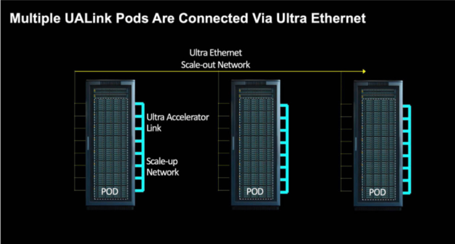
AMD contributed its broader Infinity Fabric shared memory protocol and the more limited GPU-specific xGMI to the UALink project, and all other participants agreed to use Infinity Fabric as the standard protocol for accelerator interconnection. Sachin Katti, Intel’s Senior Vice President and General Manager of the Network and Edge Business Unit, said that the “driver group” of Ultra Accelerator Link, consisting of AMD, Broadcom, Cisco Systems, Google, Hewlett Packard Enterprise, Intel, Meta Platforms, and Microsoft, is considering using the Ethernet Layer 1 transport layer and adopting Infinity Fabric on top of it to glue GPU memory into a huge shared space similar to NUMA on CPUs. As shown in the figure below, we shared how to use Ethernet to link Pods to larger clusters:
As thenextplatform said, no one expects to connect GPUs from multiple vendors within one enclosure, or possibly even within a Pod in one rack or multiple racks. But UALink alliance members do believe that system manufacturers will create machines using UALink and allow accelerators from many participants to be placed in these machines as customers build their pods. You can have a Pod with AMD GPUs, a Pod with Intel GPUs, and another with custom accelerators from any number of other participants. It allows universality of server design at the interconnect level, just as the Open Accelerator Module (OAM) specification published by Meta Platforms and Microsoft allows universality of accelerator slots on system boards.
The core advantage of UALink lies in providing opportunities for the industry to synchronize with NVIDIA technology. NVIDIA has mastered the manufacturing capability of NVSwitch boxes and has integrated them into products such as NVIDIA DGX GB200 NVL72, demonstrating strong technical prowess. Intel’s AI accelerators have annual sales of hundreds of millions of dollars, with tens of thousands expected to be sold. AMD’s MI300X, despite billions of dollars in sales, still lags behind NVIDIA. UALink technology helps companies like Broadcom manufacture switches, assisting enterprises in scaling AI and achieving efficient interconnection of accelerators from multiple companies. Technological innovation drives the flourishing development of the AI industry.
Broadcom Atlas switches plan to compete with AMD Infinity Fabric AFL Scale Up and NVIDIA NVLink, indicating they will be equipped on PCIe Gen7 switches. It is reported that this technology may achieve UALink V1.0, although the specification has not yet been officially released. This move marks Broadcom’s active positioning in the field of high-performance interconnect technology, worthy of close attention within and outside the industry.
The UALink 1.0 version specification is about to be launched in the third quarter of 2024, supporting AI container group connections of up to 1,024 accelerators, enabling direct loading and storage between accelerator (such as GPU) memories. The UALink alliance has been established and is expected to be formally operational in the same quarter, with this specification open to alliance members. This specification will greatly promote AI computing efficiency, leading a new industry standard.
ARM architecture, as a globally popular processor architecture, has cultivated multiple classic, embedded, and application processor series through years of deep cultivation. Among them, the ARM Cortex series, as an upgrade to ARM11, widely serves different markets, based on ARMv7 or ARMv8 architecture, subdivided into Cortex-A, Cortex-R, and Cortex-M three major series, continuously providing customers with excellent performance and reliable service.
UCIe (Universal Chiplet Interconnect Express) is an open chiplet interconnect standard jointly launched by industry giants AMD, Arm, Google Cloud, Intel, Qualcomm, TSMC, ASE, Samsung, etc. It aims to break down manufacturer barriers, simplify chiplet interoperability, and promote the widespread application of technology. The key features of UCIe focus on improving the interconnection efficiency and compatibility of chiplet technology, injecting new momentum into industry development.
UCIe enables seamless interconnection of chiplets from different vendors through common physical layer, protocol layer, and software stack specifications, whether within the same package or across packages. This innovation promotes modularity and flexibility in chip design, significantly reducing design complexity and cost, bringing revolutionary changes to the industry.
Multi-source compatibility is excellent, compatible with 2.5D and 3D packaging technologies, seamlessly connecting chiplets from various foundries and packaging companies, ensuring efficient interoperability and achieving seamless cross-source integration.
High-performance interconnection achieves high bandwidth and low latency, flexibly configuring various bandwidths, fully supporting multiple scenarios such as high-performance computing, data centers, mobile, and edge computing.
Security is excellent, integrating a security framework covering authentication, encryption, and data integrity protection, ensuring secure communication between chips, which is crucial for applications such as cloud services and data centers.
With standardized interfaces, UCIe simplifies the design and testing process of chiplets, allowing rapid verification and accelerating product market entry. Developers can easily utilize the best combination of chiplets to build customized system-on-chip (SoC), achieving efficient development and flexible customization.
The release of the UCIe standard leads the chip industry towards a new era of modularity and heterogeneous integration, promoting design innovation, reducing development costs, and accelerating the commercialization of new technologies. This move has profound implications for improving system performance and energy efficiency in fields such as AI, high-performance computing, and data centers.
The UCIe specification is deeply inspired by Intel’s AIB technology, which was donated to the CHIPS Alliance in 2020. The UCIe specification comprehensively covers the physical layer, communication electrical signal standards, number of channels and contact pitch, and defines higher-order protocols and necessary function sets, demonstrating strong compatibility and flexibility.
Although UCIe does not specify the physical connection packaging and bridging technology between chiplets, it allows working together through various methods such as silicon intermediary layers. As long as chiplets conform to the UCIe standard, regardless of packaging or bridging methods, they can communicate with another UCIe-supporting chiplet, demonstrating a high degree of flexibility and compatibility.
The middle layer manages link states and negotiates parameters through Die to Die adaptation units, and adds CRC cyclic redundancy check codes and link-level retry functions, providing double reliability assurance for data transmission.
Manufacturers will enjoy multiple choices at the protocol layer, especially the CXL (Compute Express Link) standard, an innovative technology derived from PCIe, bringing broader standardized support to the industry.
The UCIe organization declares that technology sources are not limited to PCIe and CXL standards, and will flexibly choose other interconnect protocols as needed, ensuring technological frontier and diversity.
Although UCIe primarily focuses on chiplet interconnection, it also supports off-chip connections. Chip and system manufacturers can build remote communications using UCIe, and although this sacrifices latency and power, it can achieve rack-to-rack server communication, and even optical interconnection, bringing innovative solutions to the industry.
The UCIe 1.0 specification marks the beginning of a new era, focusing on the physical layer and communication protocols, mainly applicable to 2D and 2.5D chip packaging. Although it appears basic when facing AMD’s Infinity Fabric or Intel’s Foveros Direct 3D technology, for most manufacturers, achieving efficiency and cost optimization through IP chip procurement and interconnection of chips with different processes remains highly attractive.
Since its release, UCIe has gained support from giants such as Google, Microsoft, Meta, with ASE Group and Qualcomm also joining, forming a strong alliance lineup. However, NVIDIA is not among them. At GTC2022, NVIDIA introduced NVLink-C2C technology, achieving interconnection between GPUs and CPUs, uniquely building its own interconnect system, on par with AMD IF and Intel Foveros, demonstrating its technical prowess and innovation spirit.