Backside Power Delivery Network (BSPDN): Revolutionizing Semiconductor Manufacturing
Introduction to Backside Power Delivery Networks
In the rapidly evolving semiconductor industry, power delivery networks are critical components that provide power supply and reference voltage to active devices on silicon chips. Traditionally, these networks have been implemented on the frontside of silicon wafers, sharing space with signal networks. However, as transistor dimensions continue to shrink into the angstrom era (18A, 14A, etc.), conventional approaches face increasing challenges related to interconnect resistance, power loss, and limited routing resources.
Enter the Backside Power Delivery Network (BSPDN) – a groundbreaking architectural innovation that fundamentally changes how power is distributed in advanced semiconductor devices.
What Is Backside Power Delivery Network Technology?
The BSPDN represents a paradigm shift in chip architecture, routing power lines through the backside of the silicon wafer rather than the traditionally used frontside. This revolutionary approach:
- Decouples the power delivery network from the signal network
- Reserves the frontside exclusively for signal routing and active device regions
- Enables direct power delivery to standard cells through wider, less resistive metal lines
- Eliminates the need for electrons to travel through the complex back-end-of-line (BEOL) stack
This architectural transformation offers significant advantages for next-generation chips, particularly as traditional FinFET architecture approaches its scaling limits.
Key Benefits of BSPDN Implementation
Performance Improvements
Samsung Electronics’ foundry business reports that implementing BSPDN technology can reduce 2nm chip size by approximately 17% compared to traditional frontside power delivery approaches. Additionally, the technology boosts performance by 8% and enhances power efficiency by 15%.
Technical Advantages
- Reduced IR Drop: By delivering power directly from below the transistors through wider, less resistive metal lines
- Improved Power Integrity: Decoupling power and signal networks leads to more stable voltage delivery
- Enhanced Thermal Management: Better heat dissipation capabilities compared to traditional approaches
- Reduced Routing Congestion: Alleviates congestion on frontside metal layers
- Smaller Standard Cell Size: Enables further standard cell height reduction, equivalent to up to two generations of lithography scaling
- Superior Efficiency: Simulation studies by Arm and Imec indicate BSPDN can be 7X more efficient than frontside power delivery
Essential Building Blocks of BSPDN Technology
Two critical technology enablers make BSPDN possible:
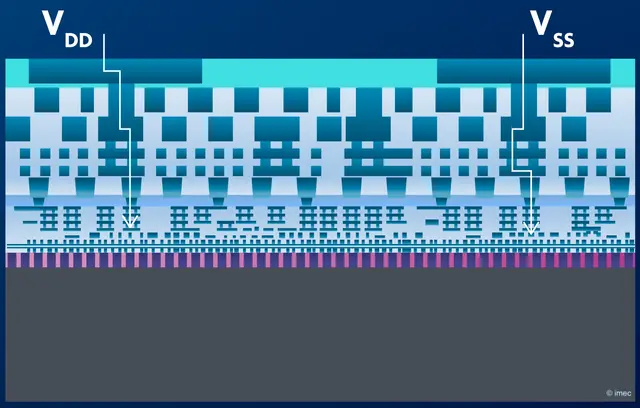
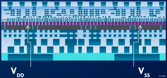
Buried Power Rails (BPRs)
BPRs are metal line constructs buried below the transistors, partially within the silicon substrate and partially within the shallow trench isolation oxide. They replace the traditional VDD and VSS power rails that were previously implemented in the BEOL at the standard cell level. This shift from BEOL to front-end-of-line (FEOL) reduces the number of metal interconnect (Mint) tracks, enabling further standard cell shrinkage.
Nano-Through-Silicon Vias (nTSVs)
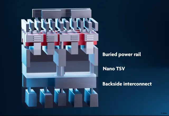
nTSVs are high-aspect-ratio vias processed in the thinned wafer’s backside. When combined with BPRs, they create an efficient path for delivering power from the wafer’s backside directly to the active devices on the frontside, maximizing IR drop reduction.
Manufacturing Challenges and Process Flow
Despite its clear benefits, implementing BSPDN introduces significant manufacturing challenges:
Wafer Processing Complexities
- Extreme Wafer Thinning: The process requires thinning the wafer to less than 500nm, a precision engineering challenge
- Wafer-to-Wafer Bonding: The device wafer must be flipped and bonded to a carrier wafer
- SiGe Etch Stop Layer: A precisely engineered SiGe layer is required for controlled wafer thinning
- High-Aspect-Ratio Via Formation: Creating nTSVs with sufficient density and precision
- Material Selection: Conventional copper faces limitations in these advanced structures, necessitating exploration of alternative metals like ruthenium, tungsten, or molybdenum
Process Flow Overview
The manufacturing process typically follows these key steps:
- Frontside Processing with Buried Rails: Creating device structures and BPRs
- Wafer-to-Wafer Bonding and Thinning: Bonding the active wafer frontside to a carrier wafer, followed by extreme thinning
- Backside Processing: Creating nTSVs that connect to the buried power rails
- Backside Metallization: Implementing the backside power distribution network
Industry Adoption and Future Outlook
Leading chipmakers are racing to implement this advanced technology:
- Intel: Positioned to be the first to implement BSPDN (branded as “PowerVia”) in its 20A (2nm) node process, coinciding with its transition to RibbonFET transistors
- Samsung: Planning to apply BSPDN to mass production of its 2nm process beginning in 2027
- TSMC: Intending to introduce BSPDN to its 1.6nm and smaller process nodes around late 2026
The semiconductor industry stands at a crucial inflection point, with two major paradigm shifts occurring simultaneously: gate-all-around (GAA) transistors and backside power delivery networks. These technologies represent the first major interconnect evolution since the shift from aluminum to copper in 1997.
Applications Beyond Traditional Chips
While BSPDN was initially conceived for advanced logic nodes, its potential extends to 3D system-on-chip (SoC) applications. In memory-on-logic configurations, where memory macros are placed on a top die and logic on a bottom die, the backside of the logic wafer can be utilized for power delivery to power-hungry core logic circuits, offering significant performance benefits.
Conclusion
Backside Power Delivery Network technology represents one of the most significant architectural innovations in semiconductor manufacturing in decades. As transistor scaling continues to push physical limits, BSPDN offers a promising solution to address mounting challenges in power delivery, performance, and chip density. While manufacturing complexities remain, the industry’s commitment to overcoming these hurdles underscores BSPDN’s critical role in the future of semiconductor technology.
The successful implementation of BSPDN could potentially reshape the competitive landscape among foundry leaders, creating new opportunities for innovation and advancement in semiconductor design and manufacturing.