Efficient Control: Analogy Semiconductor DR7808 Applications in New Energy Vehicles
Keywords: Electric vehicle, motor pre-drive, motor drive, integrated IC, multi-motor control, technological innovation
I. Eight Half-Bridge Motor Driver DR7808: Addressing Cutting-Edge Motor Drive Challenges
In the field of new energy vehicles, as the degree of vehicle electrification deepens, motor pre-drive technology faces unprecedented challenges. Traditional motor control methods, such as combinations of discrete components and relays, are gradually showing limitations, unable to meet new industry demands for high performance, cost efficiency, compact size, safety, and multi-functionality. Against this backdrop, Analogy-Semi has introduced the DR7808 eight half-bridge motor driver chip, aimed at addressing industry pain points and driving technological progress.
Compared to international competitors, the DR7808 not only comprehensively covers basic functions but also conducts in-depth optimization and enhancement in multiple aspects, including support for 4-channel PWM signal input, fine-tuning of overcurrent protection thresholds, intelligent switching of high-low side drive modes, strengthening of upper and lower switch handshake logic, and offline diagnostics with online current detection. These innovative designs not only meet customer demands for flexible application design but also ensure system stability and safety.
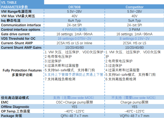
Table 1: Comparison of DR7808 with mainstream international competitors
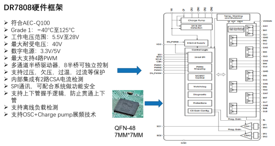
Table 2: DR7808 product parameters and hardware framework
II. DR7808 Performance Features and Technical Innovations
2.1 PWM4 Function and Application: Four-Channel PWM Drive Covering More Application Scenarios
For seat memory functions and other applications requiring coordination of four motors working simultaneously, the DR7808’s EN_PWM4 pin demonstrates its unique advantage. By cleverly setting the HB6_PWM4_EN bit in the CSA_OC_SH register, EN_PWM4 can be converted into a fourth PWM input, specifically used to drive the HB6 bridge arm. This design breakthrough breaks industry boundaries, significantly different from competitors supporting a maximum of only three PWM channels, opening new possibilities for multi-motor synchronous control.
As shown in the diagrams below, we briefly outline the configuration process and signal flow for PWM forward and reverse control. By mapping the EN_PWM4 pin to HB6, the HS and LS within HB6 can be converted to active MOSFETs according to the HB6_MODE register settings, thereby achieving forward and reverse operations under PWM drive. When HB6 is driven by the EN_PWM4 signal, the charging and discharging process of external MOSFETs is finely managed, and the static current for this process is precisely controlled by the HB6ICHGST bit in the ST_ICHG register.
It is worth noting that the EN_PWM4 pin serves as the chip enable role in its default state. Once the HB6_PWM4_EN bit is activated, the chip will not enter a disabled state even if the EN_PWM4 pin is pulled low. Under normal applications, the EN_PWM4 pin can be reset as chip enable by reconfiguring HB6_PWM4_EN to low via SPI. Meanwhile, VDD power down or watchdog timeout will reset HB6_PWM4_EN, and the EN_PWM4 pin will resume its enabling responsibility. Subsequently, when the EN_PWM4 pin is asserted low again, the chip will perform a reset operation. To ensure system stability and reliability, a recommended software practice is to read the 0x00 register three consecutive times before feeding the watchdog; if the read data is completely consistent all three times, it is considered a successful watchdog feed; conversely, if this condition is not met, the EN_PWM4 pin needs to be set to high to prevent unexpected resets caused by subsequent watchdog timeout.
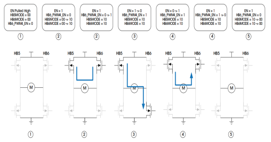
Figure 1: Forward PWM operation example
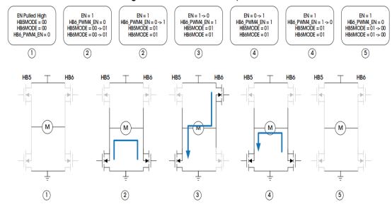
Figure 2: Reverse PWM operation example
2.2 Gate Drive and Overcurrent Protection: Fine Adjustment and Cost Optimization
The DR7808 chip demonstrates excellent performance in gate drive current regulation and overcurrent protection. Its overcurrent protection threshold covers a wide range from 0.075V to 2V, offering 16 levels of fine adjustment, which significantly outperforms competitors’ 8-level adjustment range of 0.15V to 2V, allowing the DR7808 to exhibit outstanding adaptability and safety in low-current applications.
Moreover, each gate driver in the DR7808 can precisely control current variations from 1.0mA to approximately 100mA through 32 levels, directly challenging the traditional practice of changing edge slopes by connecting resistors of different values in series in the gate drive loop to reduce current spikes when the MOS turns on. This innovative design of the DR7808 requires no additional resistors, reducing the number of peripheral components, thereby lowering costs, simplifying the design process, and making debugging work more convenient.
The DR7808 chip achieves precise control of charging and discharging currents for active MOSFETs and freewheeling MOSFETs in its gate driver design, with specific configuration steps as follows:
- Initialization configuration: First, determine the control register group to be accessed by setting the REG_BANK bit in the GENCTRL1 register.
- Active MOSFET current control: Charging current: Precisely set the charging current for active MOSFETs using the PWM_ICHG_ACT register (when REG_BANK=0).
- Discharging current: Configure the discharging current for active MOSFETs through the PWM_IDCHG_ACT register (also when REG_BANK=0).
Freewheeling MOSFET current control: Using the PWM_ICHG_FW register (when REG_BANK=1), simultaneously configure the charging and discharging currents for freewheeling MOSFETs, ensuring optimal performance during PWM operation.
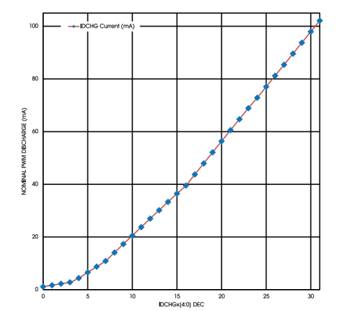
Figure 3: Configurable discharge current during PWM operation
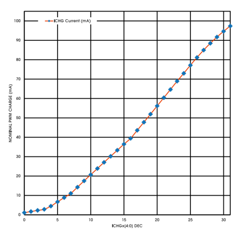
Figure 4: Configurable charge current during PWM operation
2.3 Advanced Detection and Protection Mechanisms: Ensuring H-Bridge Drive Stability and Safety
2.3.1 Upper and Lower Switch Dead Time Control and Protection Optimization
In H-bridge power drive applications, dead time control between upper and lower switches is a key element in ensuring system stability and safety. Traditional methods rely on MCU algorithms to calculate dead time, using software for control; however, the reliability of this approach is questioned under extreme conditions. For example, improper dead time settings, Cgd coupling effects on gate voltage, extreme duty cycles, and other factors may cause upper and lower switches to conduct simultaneously, leading to system failures.
To address this challenge, Analogy-Semi has introduced a series of innovative technologies in the DR7808 chip, including dynamic dead time monitoring, gate Hardoff anti-coupling, PWM duty cycle compensation, and extreme duty cycle compensation, to resolve the shortcomings of traditional methods. Users only need to set relevant parameters, and the chip’s built-in handshake detection mechanism will automatically implement internal Hardoff current strong pull-down on the lower bridge MOS through voltage logic judgment when the upper bridge MOS is turned on, ensuring that the upper and lower bridge MOSs will never turn on simultaneously under any dead time configuration, thereby achieving stable and reliable system operation.
2.3.2 Rich Diagnostic Protection Mechanism Example
The DR7808 chip is equipped with comprehensive diagnostic and protection mechanisms to address various potential failures. Taking abnormal supply voltage VM as an example, here’s how the chip responds:
- When the supply voltage VM suddenly drops from a normal value of 12V to 5V, the chip immediately triggers the undervoltage protection mechanism.
- In the data format, a Global status Byte (GEF) value of 0x08 indicates that the SUPE bit is set to 1, the chip detects a Power error, and automatically uploads the fault flag.
- At the same time, the General Status Register provides more detailed fault information, ensuring timely reporting and handling of fault status.
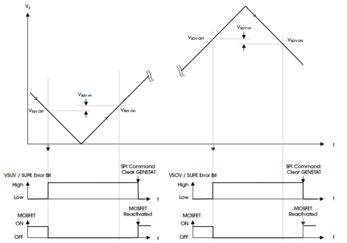
Figure 5: Output behavior under VM overvoltage and undervoltage
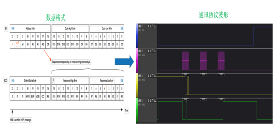
Figure 6: GEF data capture and upload during VM undervoltage
2.4 Off-brake Protection Mechanism: Safeguarding Motor and System Safety
In specific working scenarios, such as automatic tailgate adjustment or seat folding on factory assembly lines, if the battery fails to supply power to the control board in time, the back electromotive force (Back EMF) generated by the motor in motion may flow back into the power supply terminal, posing a threat to surrounding circuit elements, especially sensitive TVS (Transient Voltage Suppressors) and MOSFETs. To address this challenge, the DR7808 chip integrates an off-brake protection function, effectively mitigating this risk.
When the DR7808 chip is in passive mode, its built-in sensors continuously monitor the supply voltage VS. Once VS voltage is detected to exceed the safety threshold of 32.5V, the chip responds immediately, automatically starting MOSFETs LS4 to LS1, forcing the motor to quickly enter a braking state. This action rapidly reduces the back EMF, prevents unplanned motor rotation, and protects the system from high voltage shocks.
Subsequently, the system automatically monitors the downward trend of VS voltage until it stabilizes below 30V. At this point, the off-brake mechanism automatically releases, MOSFETs LS4 to LS1 close accordingly, and normal operation state is restored. This coherent off-brake protection process ensures that VS voltage remains within a safe range, effectively preventing TVS and MOSFETs from being damaged due to overvoltage, maintaining the stability and safety of the entire system.
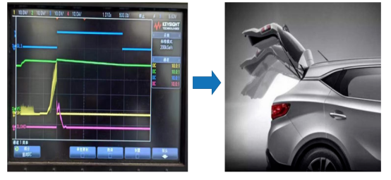
Figure 7: Off-brake protection mechanism waveform
2.5 Offline Diagnostic Mechanism: Precision Detection and Fault Troubleshooting
Through its offline state diagnostic function, the DR7808 chip can precisely detect output terminal short circuits to power, short circuits to ground, and open loads. This mechanism is ingeniously designed, providing each MOSFET’s gate driver with pull-up current (typical value 500µA) and pull-down current (typical value 1000µA) at the SHx pin when the driver is in active state (BD_PASS=0), ensuring stability and accuracy in the diagnostic process.
2.5.1 Diagnostic Steps and Principles
- MOSFET to ground short circuit detection: Set BD_PASS=0, HBx_MODE to 00b or 11b, and activate HBxIDIAG=0, while enabling internal pull-up current to pull SHx voltage close to VDRAIN. After a certain time, read the HBxVOUT register; if its value is 0b, it indicates a short circuit to ground in the MOSFET.
- MOSFET to battery short circuit detection: Similarly set BD_PASS to 0, configure HBx_MODE to 00b or 11b, but HBxIDIAG should be set to 1 to enable internal pull-down current, pulling SHx voltage close to SL. Subsequently, read the HBxVOUT register; if the read value is 1b, it indicates the MOSFET is connected to the battery, presenting a short circuit condition.
- Open load detection: This step involves detecting motor connection between HBx and HBy. First, set BD_PASS to 0, configure both HBx_MODE and HBy_MODE to 00b or 11b, set HBxIDIAG to 0 to activate pull-up current for the HBx channel, and simultaneously set HBxIDIAG for the HBy channel to 1 to enable pull-down current. After a period, read the HBxVOUT and HByVOUT registers. If the motor is normally connected, both SHx and Shy will be pulled down to SL, and both HBxVOUT and HByVOUT readings will be 0b; if the motor is disconnected, SHx will be pulled up to VDRAIN while Shy is pulled down to SL, resulting in an HBxVOUT reading of 1b and HByVOUT reading of 0b.
It is worth noting that the effective execution of the above offline detection functions requires that the bridge driver program be in active state (i.e., BD_PASS=0) and the corresponding half-bridge be in open mode (HBxMODE=00b or 11b). The pull-down current driver for each gate is activated by the control bit HBxIDIAG in the HBIDIAG register, ensuring accurate execution of the diagnostic process. When the microcontroller performs offline state diagnostics, to ensure detection accuracy, the VDSOV threshold bridger for the relevant half-bridge needs to be configured via software to a nominal value of 2V. This configuration step is key to implementing the offline diagnostic function, ensuring signal stability during detection and result reliability.
Through the above carefully designed configuration steps, the microcontroller can accurately obtain the status of HBxVOUT, efficiently and reliably completing offline diagnostic tasks, providing designers with a powerful and practical fault troubleshooting tool, enhancing the adaptability of the DR7808 chip in complex application scenarios and the convenience of system maintenance.
2.6 Precise Current Detection: Real-Time Monitoring and Optimization
The DR7808 chip internally integrates two high-precision CSA current detection op-amps, exhibiting excellent performance in offset accuracy with an error of only about 1mV, significantly outperforming international competitors. The flexibility of the chip design is reflected in its support for multiple current detection methods: it can either use a sense resistor in series at the power supply terminal, use a shunt resistor at the ground terminal, or even detect by connecting a shunt resistor in series within the motor. The unique advantage of motor terminal detection lies in its ability to monitor bidirectional current in real-time, ensuring comprehensive mastery of motor operating status.
To avoid high common-mode voltage swings at the input terminal of the current detection op-amp caused by PWM signals, it is recommended to apply PWM signals to the half-bridge terminal not connected to the shunt resistor. This layout method can effectively reduce signal interference, ensuring the accuracy and stability of current detection. As shown in Figure 8, the typical application layout of PWM and shunt resistors in the motor is presented, intuitively displaying this optimized connection strategy.
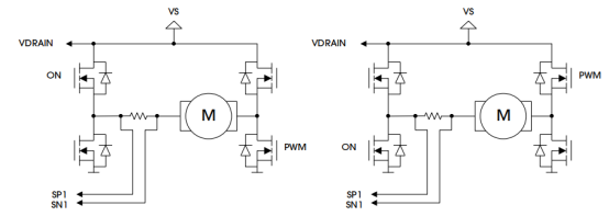
Figure 8: Diagram of PWM and shunt resistor application in the motor
In certain application scenarios, PWM signals inevitably need to be applied to the half-bridge where the shunt resistor is located. In this case, to eliminate voltage spikes in the CSA output voltage caused by high common-mode voltage jumps, the CSA PWM suppression function should be enabled by setting the CSAx_SH_EN register (x=1,2). Meanwhile, the configuration of the CSAx_SEL register needs to point to the half-bridge that needs to be sampled, ensuring that during PWM switching, the CSA output maintains the sampling state, effectively avoiding the generation of voltage spikes. The sampling and holding time is determined by tcp and tblank, further enhancing the precision and reliability of current detection.
III. DR7808: Unlimited Possibilities for Expanded Applications
The DR7808 chip demonstrates exceptional flexibility and scalability with its design of 8 independently controllable half-bridges. With independent control of upper and lower switches for each half-bridge, a single chip can support up to 4 H-bridge configurations, or flexibly configure as 8 high-side or low-side drives. This design breaks the limitations of traditional solutions, providing designers with unprecedented freedom, especially in functional domain scenarios, meeting the needs for numerous high-side or low-side drives.
In traditional applications, numerous high-side drives typically rely on discrete components, such as combinations of Darlington transistors and relays. However, these solutions have obvious drawbacks, including large device area, short mechanical switch life, noise issues, and risks of high-voltage contact sticking, plus the need for additional circuits to implement protection functions, increasing design complexity and cost. In contrast, the highly integrated design of the DR7808 shows significant advantages, not only providing the capability of 8 high-side or low-side drives in a single chip but also building in rich protection mechanisms covering overcurrent, overvoltage, undervoltage, overtemperature, and other multiple protections. Coupled with SPI communication fault diagnosis upload mechanism, it lays a solid foundation for system-level functional safety.
In high-side and low-side applications, the DR7808 design team has specifically optimized for different scenarios; when used for high-side applications, the use of low-side MOSFETs can be omitted, and vice versa. This design consideration not only simplifies circuit layout but also significantly reduces material costs, enhancing the overall cost-effectiveness of the system. In scenarios with large numbers of high-side and low-side design requirements, the DR7808 exhibits more obvious advantages compared to international competitors, standing out in both cost control and performance.
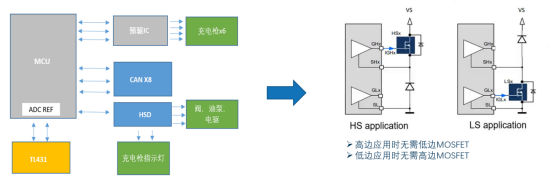
Figure 9: DR7808 design and application scenarios
IV. In conclusion
Analogy Semiconductor’s motor drive product series, with its seamless compatibility with common product BOMs on the market, not only simplifies the software design process but also ensures efficient hardware design, setting a new design standard for the industry. At the performance level, we surpass market competitors, not only leading in key indicators but also deeply excavating customer needs, introducing a series of innovative functions, directly addressing industry pain points, reshaping the technology landscape in the motor drive field.
As an outstanding representative of Analogy-Semi’s motor drive product line, the DR7808 eight half-bridge pre-drive chip, with its excellent current accuracy, enhanced handshake logic, outstanding stability, and reliability, perfectly aligns with the growing market demand for multi-motor control. In the major trend of the automotive industry moving towards intelligence and central integration, the DR7808, with its unique advantages, not only provides customers with a one-stop solution, including complete technical services such as GUI software and C language underlying drivers, but also helps customer products stand out in global competition, injecting strong power into the era of intelligent mobility.
We sincerely invite industry partners to explore the unlimited possibilities of motor drive technology together. Analogy-Semi pledges to meet challenges with a professional, innovative attitude, seize opportunities with you, and create a beautiful future for intelligent mobility. We warmly welcome your calls to discuss cooperation, let us work together to write a new chapter in the motor drive field and lead the industry towards greater achievements.