Key AI Chip Technologies: Interface IP and 3D Packaging
The rapid development of Generative Artificial Intelligence (GenAI) is profoundly changing the demand landscape for chip design, presenting unprecedented challenges for computing power, architectural design, and packaging technology.
In a recent webinar hosted by Synopsys, experts delved into the IP requirements for advanced AI chips and how GenAI is driving chip technology toward higher performance and more complex architectures.
Over the past five to six years, GenAI’s demand for computing power has increased more than ten thousand times, prompting SoC design to shift from monolithic to multi-chip architectures and driving innovation in advanced packaging technologies, high-bandwidth memory (HBM), and chip-to-chip communication.
This article will analyze in detail the impact of GenAI on chip design and explore three key technical solutions proposed by Synopsys: chip-to-chip communication, custom HBM, and 3D stacking.
The Impact of Generative AI on Chip Design
The rise of generative artificial intelligence has greatly increased the demand for computing power. Taking models in the field of Natural Language Processing (NLP) as examples, from the early GPT-3 to today’s GPT-4 and Megatron-Turing NLG, the scale of model parameters has rapidly expanded, with computing demands growing exponentially.
In the past five to six years, GenAI’s computing demands have grown by more than 10,000 times. The extremely high requirements of AI applications for chip performance have forced chip designers to break through traditional technical limitations and develop chips capable of supporting ultra-large-scale parallel computing.
This growth in demand is reflected not only in the number of computing cores but also in higher requirements for data throughput and energy efficiency. For example, training a large language model may require thousands of GPUs or TPUs running in parallel for months, consuming computational resources far beyond traditional applications. Chip design must achieve comprehensive improvements in process technology, architecture optimization, and power management.
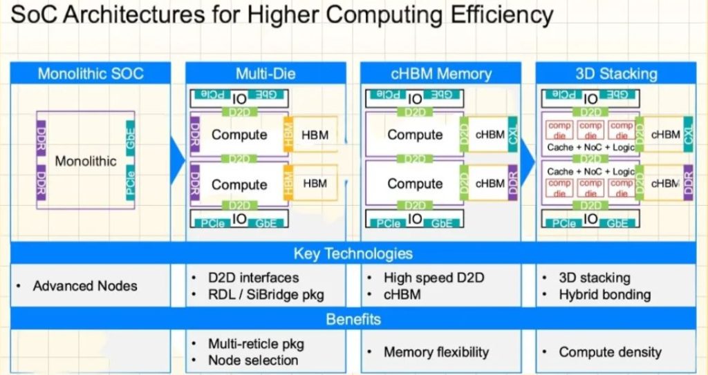
From Monolithic to Multi-Chip Architecture
Traditional monolithic SoCs (System on Chips) integrate all functional modules on a single chip, offering advantages of simple design and lower cost. However, as transistor counts break through the trillion-level barrier, monolithic designs face numerous challenges: declining yields at advanced process nodes, excessive power consumption, and increasing heat dissipation difficulties.
GenAI’s computing demands have driven SoC design to shift from monolithic to multi-chip architecture. Multi-chip SoCs decompose functional modules into multiple independent chips (chiplets) that work collaboratively through high-speed chip-to-chip interfaces.
The advantages of this architecture lie in flexibility and performance optimization. Computing cores can adopt advanced processes such as 3nm or 5nm to enhance performance, while I/O or memory modules can use more mature 28nm or 16nm processes to reduce costs.
Additionally, multi-chip designs can effectively alleviate heat dissipation problems, improving overall system stability by dispersing heat sources.
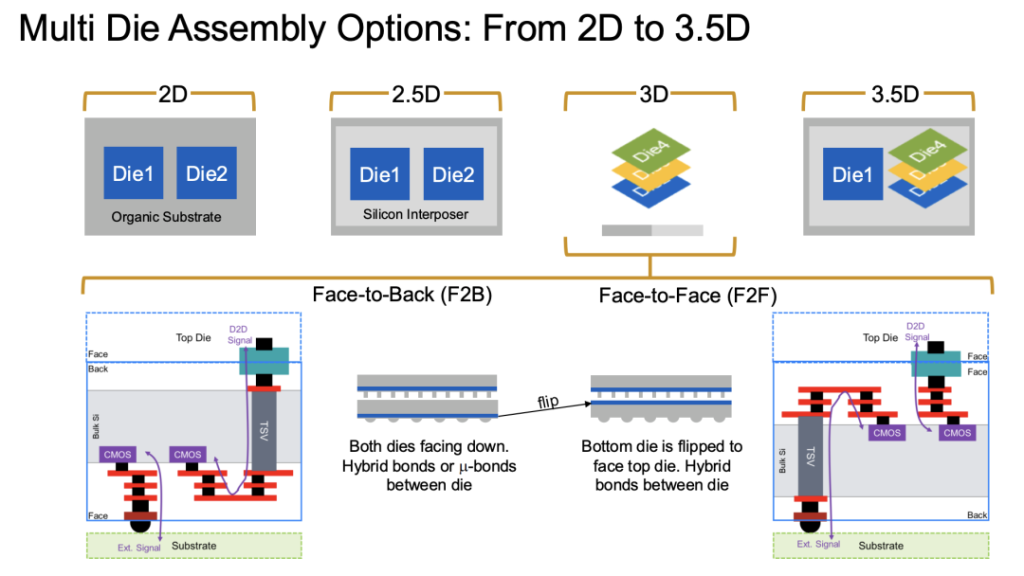
Evolution of Advanced Packaging Technologies
As chip functionality increases and computing demands rise, chip sizes continue to expand, making traditional 2D packaging technologies insufficient to meet requirements. Advanced packaging technologies are evolving from 2D and 2.5D to 3D and 3.5D.
Redistribution Layer (RDL) interposer technology enables high-density interconnections across multiple masks, becoming an important means of solving chip scaling problems.
- 5D packaging uses silicon interposers to place multiple chips side by side, providing higher bandwidth and integration.
- 3D packaging further shortens signal paths by vertically stacking chips, reducing latency and power consumption.
The application of these technologies is particularly critical in GenAI-driven high-performance SoCs, supporting the integration of larger-scale computing units and memory modules.

Memory Architecture Innovation
GenAI’s demands for memory bandwidth and capacity are equally significant, driving innovation in memory architecture.
High Bandwidth Memory (HBM) technology has become the core solution to meet this demand. By stacking multiple layers of DRAM, HBM can provide extremely high bandwidth in limited space, with HBM3 single-stack bandwidth reaching over 2TB/s.
The webinar specifically mentioned that custom HBM (cHBM) further enhances the flexibility and performance of memory architecture by integrating logic processes on base chips.
The application of memory stacking technology allows SoCs to more efficiently process large-scale datasets in GenAI tasks. For example, when training deep neural networks, chips need to quickly access large numbers of parameters and intermediate results, and HBM’s high bandwidth and low latency significantly improve data throughput.
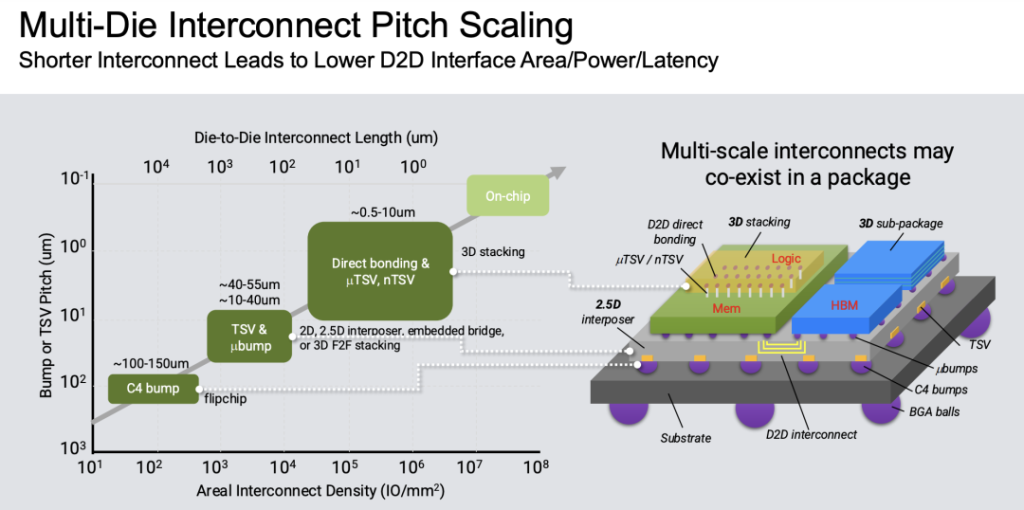
Chip-to-Chip Communication Breakthrough
The proliferation of multi-chip SoCs has made chip-to-chip communication bandwidth a key bottleneck for system performance. Chip-to-chip bandwidth is increasing from 16Gbps/pin to 32Gbps/pin, and even reaching 64Gbps/pin.
High-speed interface standards such as UCIe (Universal Chiplet Interconnect Express) have emerged, providing unified specifications for chip-to-chip communication.
Synopsys’ 64Gbps chip-to-chip communication IP solution stands out in this field, not only supporting high data rates but also featuring low-power modes and extensive testability functions. These technological advances ensure that multi-chip SoCs can work efficiently together, meeting GenAI’s stringent requirements for bandwidth and low latency.
Key Technology Analysis
Chip-to-Chip Communication
Chip-to-chip communication is the core technology of multi-chip SoCs, directly determining overall system performance. Synopsys’ 64Gbps chip-to-chip communication IP solution is optimized for proprietary systems with the following features:
- High Data Rate: Supports transmission speeds up to 64Gbps/pin, quadrupling bandwidth compared to traditional 16Gbps/pin interfaces.
- Low Power Design: Provides low-power modes and adjustable knobs to adapt to energy efficiency requirements of different application scenarios.
- Reliability and Testability: Integrates Lite FEC (Forward Error Correction) technology for low-latency error correction and supports extensive boot, debug, and reliability features.
- Modular Architecture: Flexibly adapts to different packaging technologies (such as 2D, 2.5D) and system requirements.
The UCIe standard plays a crucial role in advancing chip-to-chip communication. Synopsys’ solution extends from UCIe 40G to 64Gbps, providing higher performance and compatibility for GenAI applications. For example, in data center SoCs, these high-speed interfaces can support seamless data exchange between multiple computing chiplets, avoiding bandwidth bottlenecks.
High-speed communication also faces challenges such as signal integrity, crosstalk, and thermal management. Synopsys effectively reduces the impact of these issues through optimized PHY design and enhanced shielding techniques, ensuring the stability of communication links.
Custom HBM
Custom HBM (cHBM) technology brings revolutionary changes to SoC memory architecture. By implementing HBM customization using logic processes on base chips, Synopsys provides an efficient memory solution.
Dr. Manuel Mota pointed out that the main advantages of custom HBM include:
- Extended Usage Range: Allows multiple memory layers to share the same chip edge, reducing design complexity and cost.
- Computation Offloading: Transfers some computational tasks to chiplets, reducing the burden on the main chip and improving system efficiency.
- Technology Isolation and Scalability: Decouples host and memory technologies, facilitating future upgrades to HBM4 or other memory types.
In terms of performance, custom HBM can provide double the memory bandwidth advantage. For example, in a typical multi-chip SoC, custom HBM can work closely with computing cores through high-speed chip-to-chip links, supporting rapid access to large-scale parameters in GenAI training. This technology also enhances SoC flexibility, allowing designers to adjust memory configurations based on specific applications.
Implementing custom HBM requires solving problems such as thermal density and channel length. Synopsys ensures the stability and reliability of memory performance by optimizing the thermal design of base chips and interposer routing.
3D Stacking Technology
3D stacking technology is a key approach to realizing next-generation high-performance SoCs, significantly enhancing integration and energy efficiency through vertical integration of multiple chips.
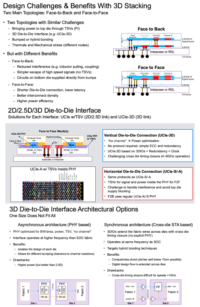
Manuel showcased commercial application cases from Intel and AMD in the webinar, such as Intel’s Foveros and AMD’s 3D V-Cache, emphasizing the importance of this technology in GenAI-driven chip design.
Compared to traditional 2D designs, 3D stacking technology excels in power savings, reducing power consumption by approximately 80%, mainly due to shorter signal paths.
Through face-to-face (F2F) or face-to-back (F2B) stacking topologies, higher chip density is achieved, greatly increasing integration levels. The design also shortens routing lengths, reducing latency, making it very suitable for AI applications requiring high bandwidth and low latency.
3D stacking technology also faces challenges, including concentrated heat issues from multi-layer stacking, requiring efficient cooling solutions to manage temperature; extremely high requirements for power stability from high-speed signals, necessitating precise decoupling designs to reduce power noise; and as interconnect spacing shrinks from 10μm to smaller dimensions, higher precision bonding techniques, such as hybrid bonding, must be adopted to ensure performance and reliability.
Synopsys’ solutions include 3D stacking IP supporting UCIe-3D interfaces, capable of achieving cross-chip timing convergence at high frequencies of 4-6GHz, providing comprehensive F2F and F2B design support, helping customers address thermal management and signal integrity challenges. In an AI training SoC, 3D stacking technology can tightly couple computing cores and caches, significantly improving data processing efficiency.
To sum up
The profound impact of generative artificial intelligence on chip design and the IP requirements trend for advanced AI chips is clear. As GenAI’s demand for computing power continues to surge, chip design is moving toward a new era of multi-chip SoCs, advanced packaging, and high-bandwidth communication.
The chip-to-chip communication, custom HBM, and 3D stacking technologies proposed by Synopsys provide viable solutions to address these challenges. With the deep development of AI applications in fields such as autonomous driving, medical imaging, and intelligent manufacturing, chip design will face higher performance and power requirements. Interface IP and 3D packaging technologies will play core roles in this process, continuously pushing chip technology beyond its limits.